Nanostructures on tungsten, SEM
Numéro d’image : 14115203
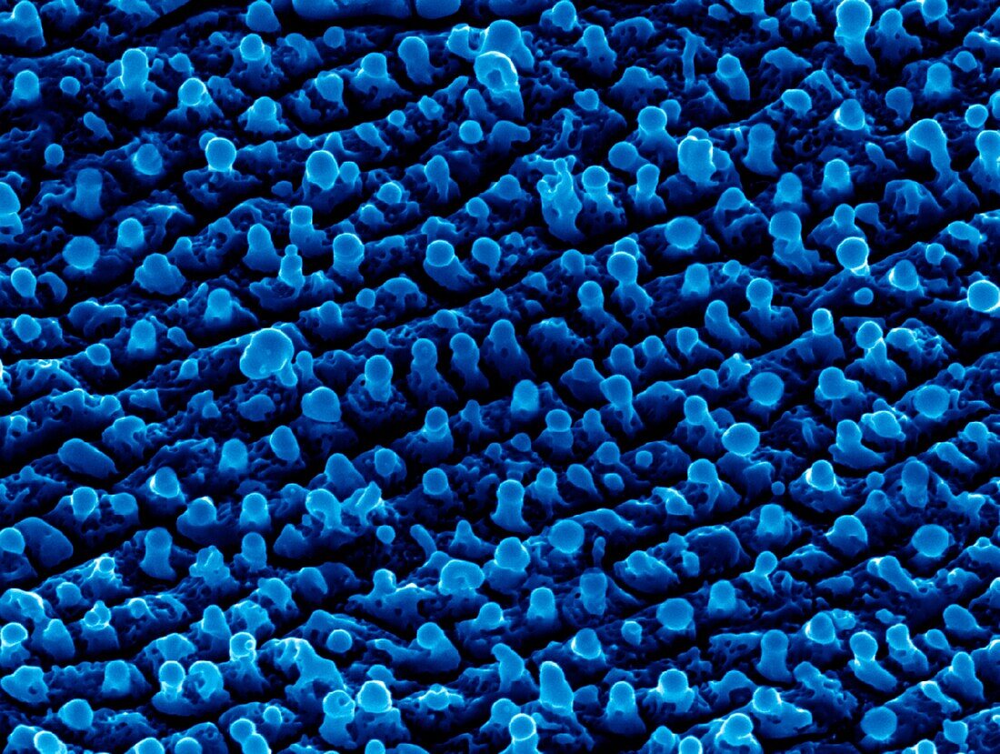
| Nanostructures on tungsten. Coloured scanning electron micrograph (SEM) of nanostructures formed on a tungsten surface by a laser beam. This research involves the use of lasers to etch and ablate metal and semiconductor surfaces. The resulting nanostructures can have applications in various forms of electronics and nanotechnology. | |
| Licence : | Libre de droits |
| Crédit: | Science Photo Library / GEORGY SHAFEEV |
| Model Release : | Non requis |
| Property Release : | Non requis |
| Restrictions : | - |
Prix pour cette image À partir de 29 €
Pour une utilisation numérique (72 dpi)
À partir de 29 €
Pour un usage d'impression (300 dpi)
À partir de 325 €