Metal crater formed by a laser, SEM
Numéro d’image : 14115195
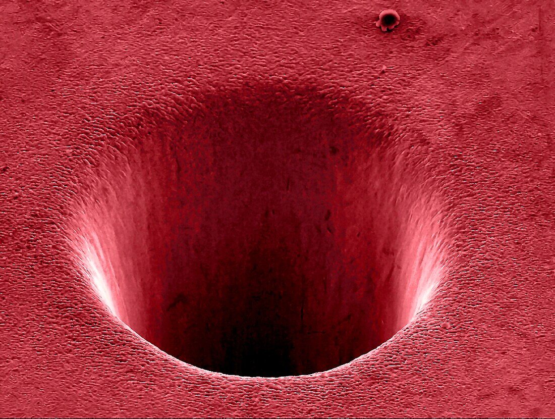
| Metal crater formed by a laser. Coloured scanning electron micrograph (SEM) of a nanoscale crater formed on a metal surface by a picosecod laser beam. This crater was produced during research that involves the use of lasers to etch and ablate metal and semiconductor surfaces. The resulting nanostructures can have applications in various forms of electronics and nanotechnology. | |
| Licence : | Libre de droits |
| Crédit: | Science Photo Library / GEORGY SHAFEEV |
| Model Release : | Non requis |
| Property Release : | Non requis |
| Restrictions : | - |
Prix pour cette image À partir de 29 €
Pour une utilisation numérique (72 dpi)
À partir de 29 €
Pour un usage d'impression (300 dpi)
À partir de 325 €