Metal crater formed by a laser, SEM
Numéro d’image : 12394538
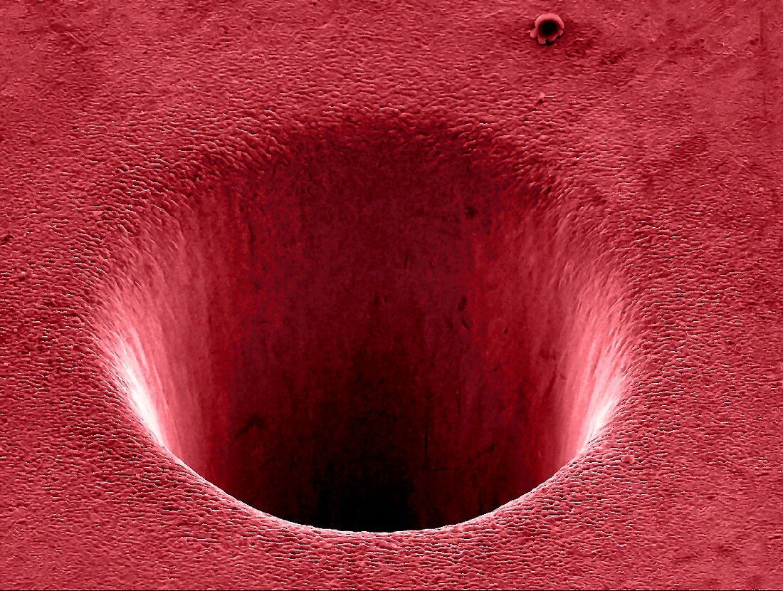
| Metal crater formed by a laser. Coloured scanning electron micrograph (SEM) of a nanoscale crater formed on a metal surface by a picosecod laser beam. This crater was produced during research that involves the use of lasers to etch and ablate metal and semiconductor surfaces. The resulting nanostructures can have applications in various forms of electronics and nanotechnology. | |
| Licence : | Droits gérés |
| Crédit: | Science Photo Library / GEORGY SHAFEEV |
| Taille de l’image : | 6805 px × 5136 px |
| Model Release : | Non requis |
| Property Release : | Non requis |
| Restrictions : | - |
Prix pour cette image À partir de 45 €
Produit vendu
(Calendrier, Carte postale, Carte de vœux, Impression sur textile, Packaging etc)
À partir de 45 €
Usage commercial
(Affichage, Annonce presse, Annonce TV, Carte, Digital - hors rés. sociaux, Digital - rés. sociaux etc)
À partir de 45 €
Éditorial
(Digital, Journal, Livre, Livre pratique, Magazine, Télévision etc)
À partir de 60 €
Usage non-commercial
(Digital - hors rés. sociaux, Digital - rés. sociaux etc)
À partir de 120 €