GaAs wafer to make superconductor being tested
Numéro d’image : 12073003
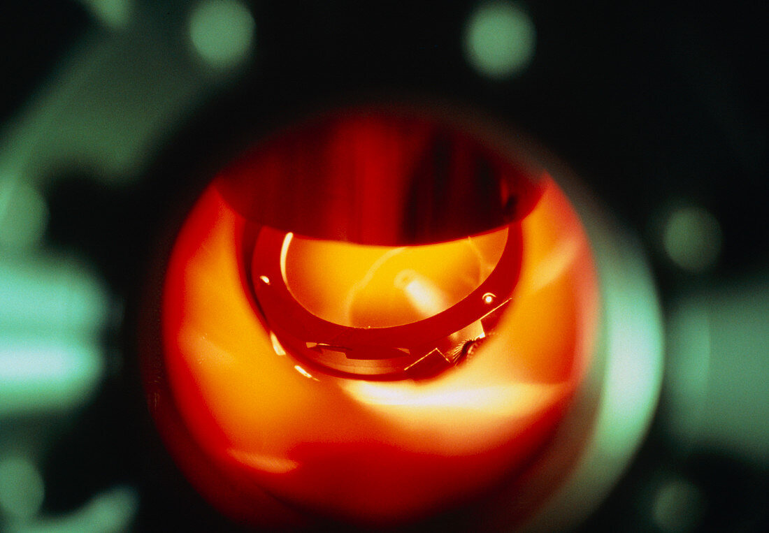
| A gallium arsenide (GaAs) wafer being heated inside a scanning auger electron spectrometer. This machine tests the wafer for purity before it is passed through the superconductor manufacturing process. The wafer will later be placed in a molecular beam epitaxy system,where molecules of various elements are implanted into the GaAs lattice structure | |
| Licence : | Droits gérés |
| Crédit: | Science Photo Library / Luria, Dick |
| Taille de l’image : | 5253 px × 3642 px |
| Model Release : | Non requis |
| Property Release : | Non requis |
| Restrictions : |
|
Prix pour cette image À partir de 45 €
Produit vendu
(Calendrier, Carte postale, Carte de vœux, Impression sur textile, Packaging etc)
À partir de 45 €
Usage commercial
(Affichage, Annonce presse, Annonce TV, Carte, Digital - hors rés. sociaux, Digital - rés. sociaux etc)
À partir de 45 €
Éditorial
(Digital, Journal, Livre, Livre pratique, Magazine, Télévision etc)
À partir de 60 €
Usage non-commercial
(Digital - hors rés. sociaux, Digital - rés. sociaux etc)
À partir de 120 €
Mots clés
- arséniure de gallium,
- arséniure gallium,
- circuit intégré,
- de pointe,
- électron,
- électronique,
- fabrication de puces,
- fabriquer,
- haute technologie,
- industrie des semi-conducteurs,
- industrie des semiconducteurs,
- manufacturer,
- plaquette,
- puce,
- spectromètre,
- supraconducteur,
- technologie,
- usine de fabrication de puces