Fabrication of silicon-based integrated circuits
Numéro d’image : 11894733
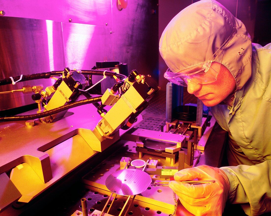
| Fabrication of silicon-based integrated circuits (chips),showing a technician monitoring the progress of low-temperature,plasma-enhanced nitride passivation,performed to protect the metal interconnect layer on the chip. Individual chips are constructed on a single wafer of crystalline silicon (visible at bottom centre). The complicated pattern of embedded layers and zones which comprises each integrated circuit was created by successive imaging,etching and deposition or growth processes. This particular wafer consists of chips that will be used to control the motors in computer disk drives | |
| Licence : | Droits gérés |
| Crédit: | Science Photo Library / SEAGATE MICROELECTRONICS LTD / DAVID PARKER |
| Taille de l’image : | 4736 px × 3766 px |
| Model Release : | Le droit n'est pas encore disponible. Merci de nous contacter avant utilisation. |
| Property Release : | Non requis |
| Restrictions : | - |
Prix pour cette image À partir de 45 €
Produit vendu
(Calendrier, Carte postale, Carte de vœux, Impression sur textile, Packaging etc)
À partir de 45 €
Usage commercial
(Affichage, Annonce presse, Annonce TV, Carte, Digital - hors rés. sociaux, Digital - rés. sociaux etc)
À partir de 45 €
Éditorial
(Digital, Journal, Livre, Livre pratique, Magazine, Télévision etc)
À partir de 60 €
Usage non-commercial
(Digital - hors rés. sociaux, Digital - rés. sociaux etc)
À partir de 120 €