Visual inspection of photomask
Numéro d’image : 11894727
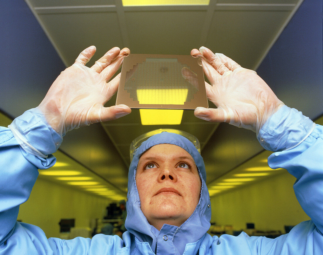
| Visual inspection of a photomask used in the fabrication of integrated circuit wafers at Seagate Microelectronics Ltd,Livingston,Scotland. The photomask is used in a photolithography process to selectively etch an electronic pattern onto a wafer of crystalline silicon - the base material for the ultimate integrated circuits that will be die stamped from the completed wafer | |
| Licence : | Droits gérés |
| Crédit: | Science Photo Library / SEAGATE MICROELECTRONICS LTD / DAVID PARKER |
| Taille de l’image : | 3732 px × 2954 px |
| Model Release : | Le droit n'est pas encore disponible. Merci de nous contacter avant utilisation. |
| Property Release : | Non requis |
| Restrictions : | - |
Prix pour cette image À partir de 45 €
Produit vendu
(Calendrier, Carte postale, Carte de vœux, Impression sur textile, Packaging etc)
À partir de 45 €
Usage commercial
(Affichage, Annonce presse, Annonce TV, Carte, Digital - hors rés. sociaux, Digital - rés. sociaux etc)
À partir de 45 €
Éditorial
(Digital, Journal, Livre, Livre pratique, Magazine, Télévision etc)
À partir de 60 €
Usage non-commercial
(Digital - hors rés. sociaux, Digital - rés. sociaux etc)
À partir de 120 €