Scientist inspecting special coating system
Numéro d’image : 11894724
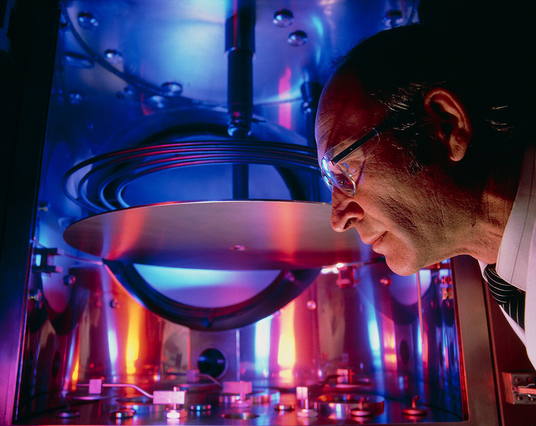
| Scientist inspecting a component of a special coating system under development in the laboratory at Edwards High Vacuum (a member of The BOC Group) Crawley,U.K. High vacuum technology is a requirement of the semiconductor industry. Vacuum chambers are used to deposit thin metallic films onto silicon wafers during the manufacture of individual integrated circuits (silicon chips). Circular silicon wafers,typically 2-3 inches in diamter are used as the building-blocks of the "chips",which are diced from the completed wafers | |
| Licence : | Droits gérés |
| Crédit: | Science Photo Library / Fielding, Malcolm / The Boc Group |
| Taille de l’image : | 4724 px × 3759 px |
| Model Release : | Le droit n'est pas encore disponible. Merci de nous contacter avant utilisation. |
| Property Release : | Non requis |
| Restrictions : | - |
Prix pour cette image À partir de 45 €
Produit vendu
(Calendrier, Carte postale, Carte de vœux, Impression sur textile, Packaging etc)
À partir de 45 €
Usage commercial
(Affichage, Annonce presse, Annonce TV, Carte, Digital - hors rés. sociaux, Digital - rés. sociaux etc)
À partir de 45 €
Éditorial
(Digital, Journal, Livre, Livre pratique, Magazine, Télévision etc)
À partir de 60 €
Usage non-commercial
(Digital - hors rés. sociaux, Digital - rés. sociaux etc)
À partir de 120 €