Manufacture of semi-conductor wafers
Numéro d’image : 11894721
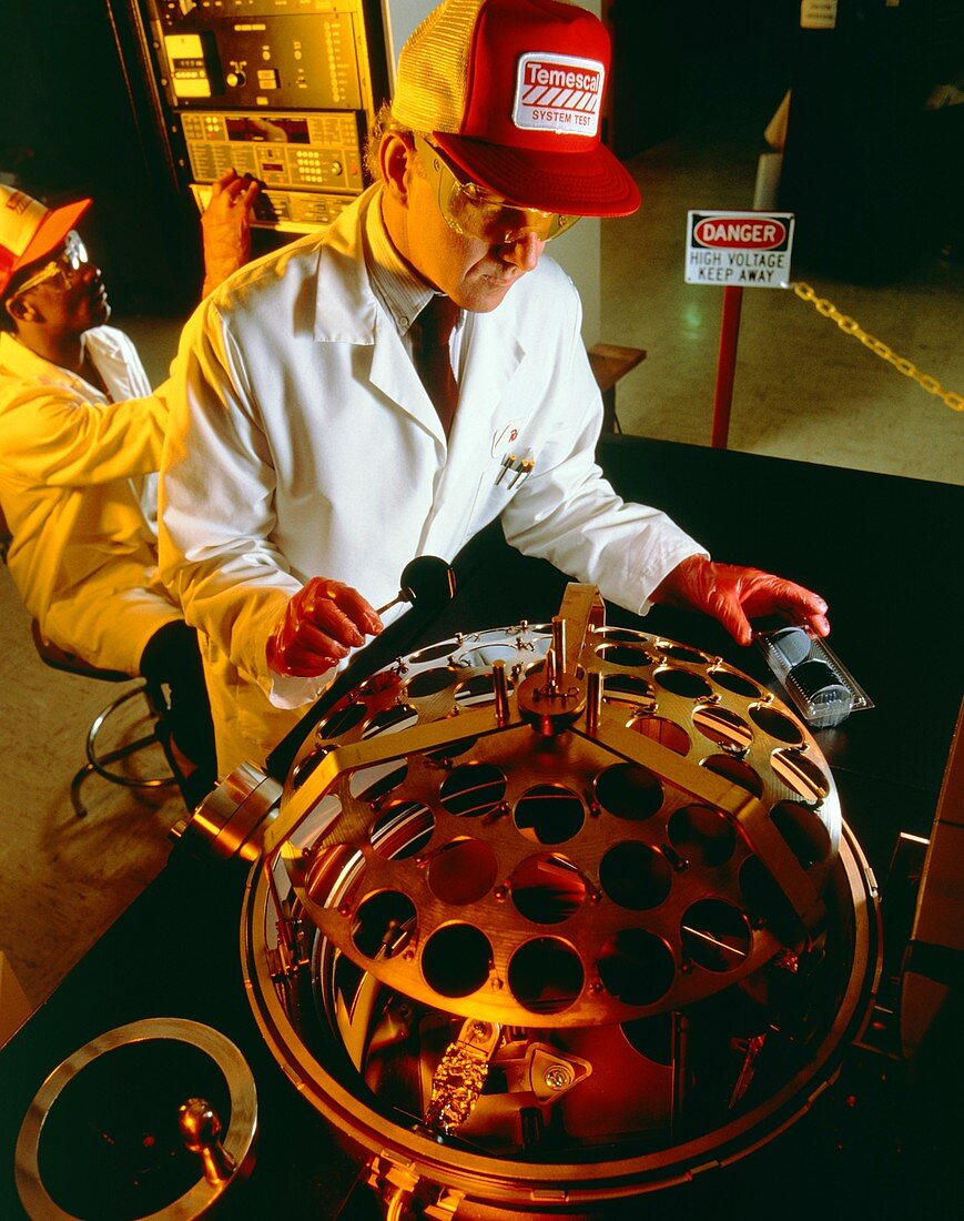
| Stage in the manufacture of high-performance semiconductor wafers: an engineer loads 2-inch diameter gallium arsenide (GaAs) wafers onto a planetary mounting for a FC-1800 fast-cycle coater,a sputtering system that deposits thin metallic films onto the wafer. Semiconductor wafers are the building-blocks of individual integrated circuits and have traditionally been made of silicon. Chips based on GaAs are up to 10 times faster at handling data than silicon & are more resistant to corruption by radiation. Photographed at Temescal,a member of The BOC Group plc,at their plant in Berkeley,California | |
| Licence : | Droits gérés |
| Crédit: | Science Photo Library / Fielding, Malcolm / The Boc Group |
| Taille de l’image : | 3756 px × 4757 px |
| Model Release : | Le droit n'est pas encore disponible. Merci de nous contacter avant utilisation. |
| Property Release : | Non requis |
| Restrictions : | - |
Prix pour cette image À partir de 45 €
Produit vendu
(Calendrier, Carte postale, Carte de vœux, Impression sur textile, Packaging etc)
À partir de 45 €
Usage commercial
(Affichage, Annonce presse, Annonce TV, Carte, Digital - hors rés. sociaux, Digital - rés. sociaux etc)
À partir de 45 €
Éditorial
(Digital, Journal, Livre, Livre pratique, Magazine, Télévision etc)
À partir de 60 €
Usage non-commercial
(Digital - hors rés. sociaux, Digital - rés. sociaux etc)
À partir de 120 €