View of a semiconductor wafer and its chips
Numéro d’image : 11894659
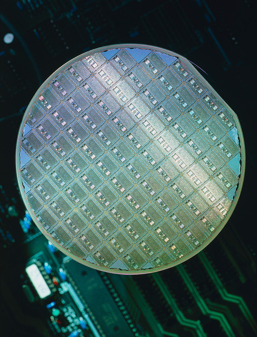
| Semiconductor wafer. View of a circular semi- conductor wafer. The surface of the wafer is covered by several blocks of integrated circuits (ICs) known as chips. The ICs are formed on the thin silicon wafer by various deposition and etching techniques. If all the individual ICs work correctly,they are cut from the wafer and placed in holders for use on circuit boards in electronic devices | |
| Licence : | Droits gérés |
| Crédit: | Science Photo Library / Knapton, Chris |
| Taille de l’image : | 3942 px × 5163 px |
| Model Release : | Non requis |
| Property Release : | Non requis |
| Restrictions : | - |
Prix pour cette image À partir de 45 €
Produit vendu
(Calendrier, Carte postale, Carte de vœux, Impression sur textile, Packaging etc)
À partir de 45 €
Usage commercial
(Affichage, Annonce presse, Annonce TV, Carte, Digital - hors rés. sociaux, Digital - rés. sociaux etc)
À partir de 45 €
Éditorial
(Digital, Journal, Livre, Livre pratique, Magazine, Télévision etc)
À partir de 60 €
Usage non-commercial
(Digital - hors rés. sociaux, Digital - rés. sociaux etc)
À partir de 120 €