Nanoparticle layer microelectronics
Numéro d’image : 12992027
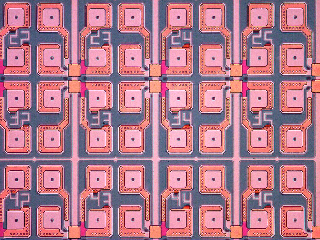
| Nanoparticle layer microelectronics. Array of metallic nanoparticle contacts developed to allow molecular monolayer electronic devices. This method allows molecular integration on conventional silicon chips, using the standard fabrication methods of the semiconductor industry. Image published in July 2018. | |
| Licence : | Droits gérés |
| Crédit: | Science Photo Library / IBM Research |
| Taille de l’image : | 3417 px × 2563 px |
| Model Release : | Non requis |
| Property Release : | Non requis |
| Restrictions : | - |
Prix pour cette image À partir de 45 €
Produit vendu
(Calendrier, Carte postale, Carte de vœux, Impression sur textile, Packaging etc)
À partir de 45 €
Usage commercial
(Affichage, Annonce presse, Annonce TV, Carte, Digital - hors rés. sociaux, Digital - rés. sociaux etc)
À partir de 45 €
Éditorial
(Digital, Journal, Livre, Livre pratique, Magazine, Télévision etc)
À partir de 60 €
Usage non-commercial
(Digital - hors rés. sociaux, Digital - rés. sociaux etc)
À partir de 120 €
Mots clés
- 2018,
- 21ème siècle,
- aucun,
- coloré,
- colorié,
- colorisé,
- couche,
- électronique,
- ensemble,
- M.E.B.,
- MEB,
- microélectronique,
- microscope électronique à balayage,
- nanoparticule,
- nanotechnologie,
- personne,
- physique,
- puce,
- puce en silicium,
- réseau,
- semi-conducteur,
- semi-conducteurs,
- semiconducteurs,
- technologie,
- technologique,
- XX1ème siècle