Hall effect, illustration
Numéro d’image : 12492439
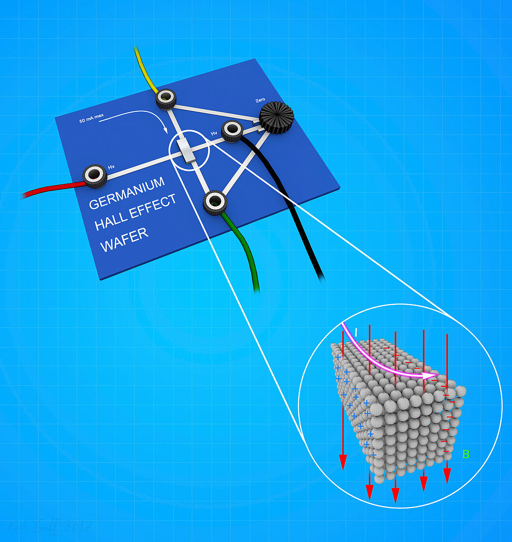
| Hall effect. Illustration of a germanium Hall effect wafer (upper left) and the resulting Hall effect in the germanium crystal (bottom right). An electrical current (pink line) is applied to the crystal and a potentiometer (ring at far right of Hall effect board) is used to balance the voltage to zero. The wafer is placed in a magnetic field perpendicular to the direction of the current. This causes a deflection in the current that leads to a negative charge building up on one side of the crystal, with a positive charge on the opposite side, and thus an electric potential is induced. This potential difference is called the Hall voltage. | |
| Licence : | Droits gérés |
| Crédit: | Science Photo Library / KARL GAFF |
| Taille de l’image : | 4066 px × 4298 px |
| Model Release : | Non requis |
| Property Release : | Non requis |
| Restrictions : | - |
Prix pour cette image À partir de 45 €
Produit vendu
(Calendrier, Carte postale, Carte de vœux, Impression sur textile, Packaging etc)
À partir de 45 €
Usage commercial
(Affichage, Annonce presse, Annonce TV, Carte, Digital - hors rés. sociaux, Digital - rés. sociaux etc)
À partir de 45 €
Éditorial
(Digital, Journal, Livre, Livre pratique, Magazine, Télévision etc)
À partir de 60 €
Usage non-commercial
(Digital - hors rés. sociaux, Digital - rés. sociaux etc)
À partir de 120 €