Scanning electron microscope
Numéro d’image : 11832531
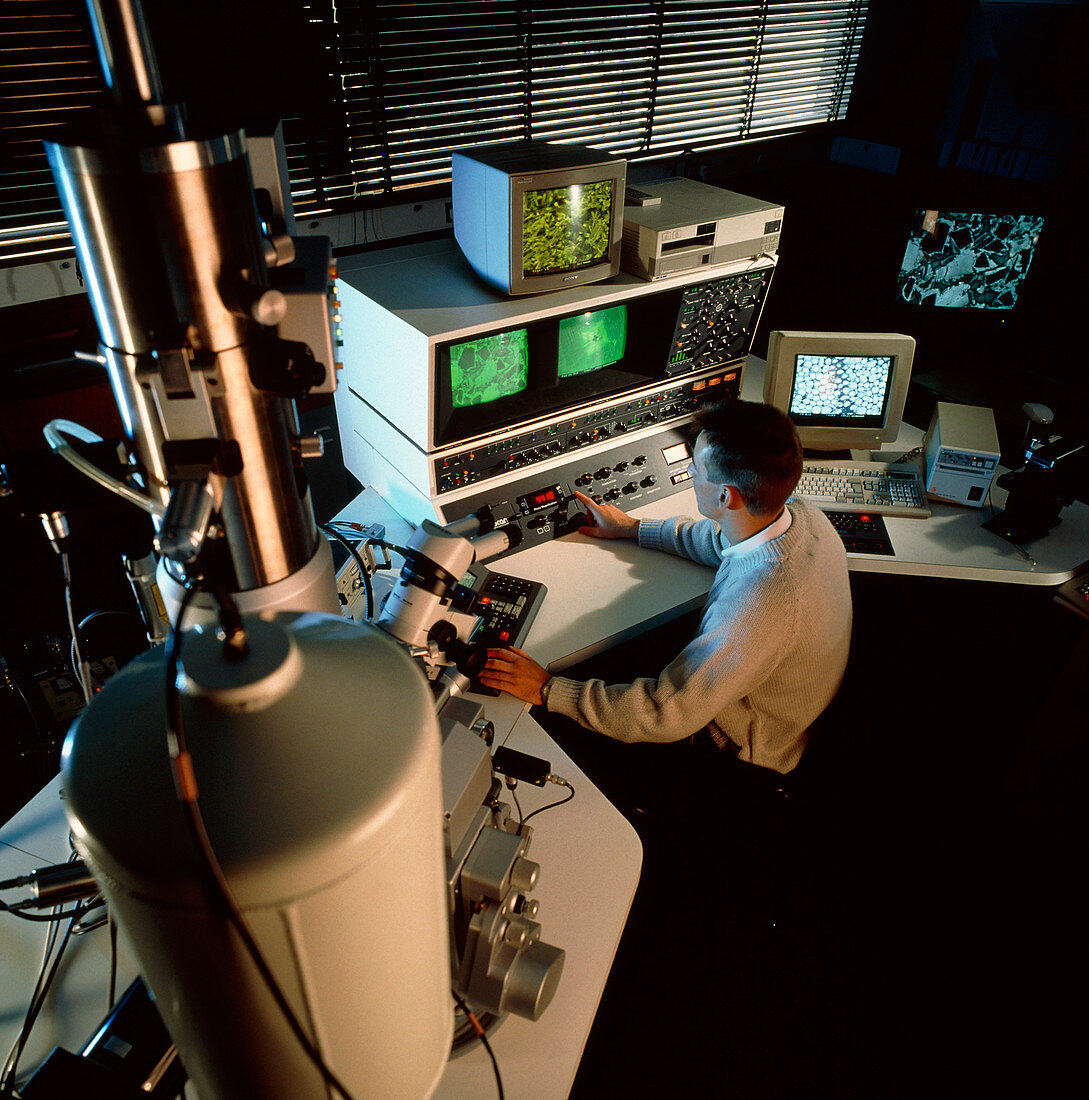
| Scanning electron microscope. Researcher using a scanning electron microscope (SEM,lower left) to study synthetic materials. SEMs use an electron beam to obtain three-dimensional images of objects. The electron beam is swept over the sample,causing secondary electrons to be emitted. These and reflected electrons are used to form the image. Seen on the screens are,from left to right: silicon carbide ceramic,alumina ceramic strengthened with silicon carbide (top),damaged light-emitting sample of magnesium oxide,low- friction surface for textiles,magnified 5000 times,and another silicon carbide ceramic. Photo- graphed at the University of Newcastle,England | |
| Licence : | Droits gérés |
| Crédit: | Science Photo Library / Cuthbert, Colin |
| Taille de l’image : | 3506 px × 3543 px |
| Model Release : | Le droit n'est pas encore disponible. Merci de nous contacter avant utilisation. |
| Property Release : | Non requis |
| Restrictions : | - |
Prix pour cette image À partir de 45 €
Produit vendu
(Calendrier, Carte postale, Carte de vœux, Impression sur textile, Packaging etc)
À partir de 45 €
Usage commercial
(Affichage, Annonce presse, Annonce TV, Carte, Digital - hors rés. sociaux, Digital - rés. sociaux etc)
À partir de 45 €
Éditorial
(Digital, Journal, Livre, Livre pratique, Magazine, Télévision etc)
À partir de 60 €
Usage non-commercial
(Digital - hors rés. sociaux, Digital - rés. sociaux etc)
À partir de 120 €